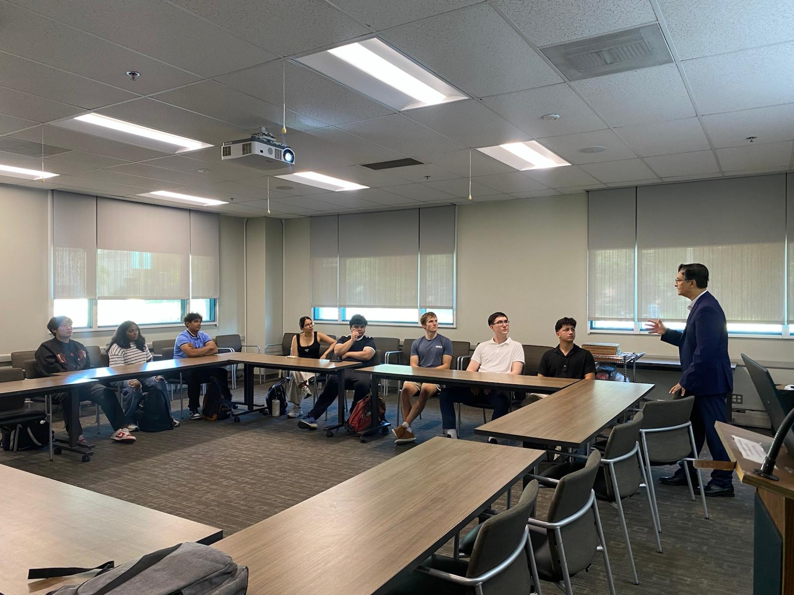
Summer AI & Semiconductor Internship Program
The Northwest AI Hub has received over 100 applications for our upcoming Summer AI and Semiconductor Internship Program. Applicants include students from UC Davis, Sacramento State University, and community colleges in the Sacramento and Stockton areas. Selected interns will have the opportunity to work with UC Davis professors in various disciplines, including:
- Electronic & Photonic Devices
- System & AI on Chip
- Semiconductor Fabrication
- Chip Design
- Device Physics
- Semiconductor-Related Material Science
- Semiconductor Testing, Measurement & Analysis
K-12 programs
Spring K-12 Workshop Activity
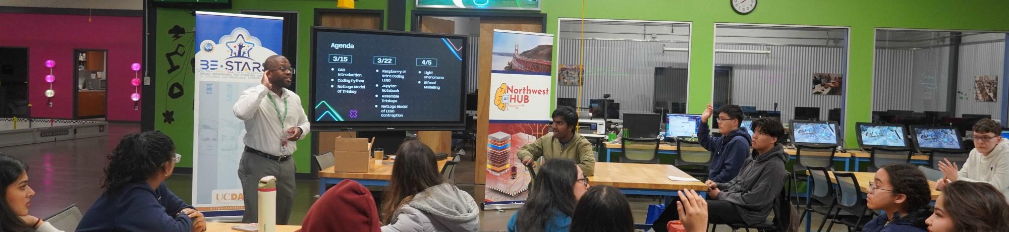
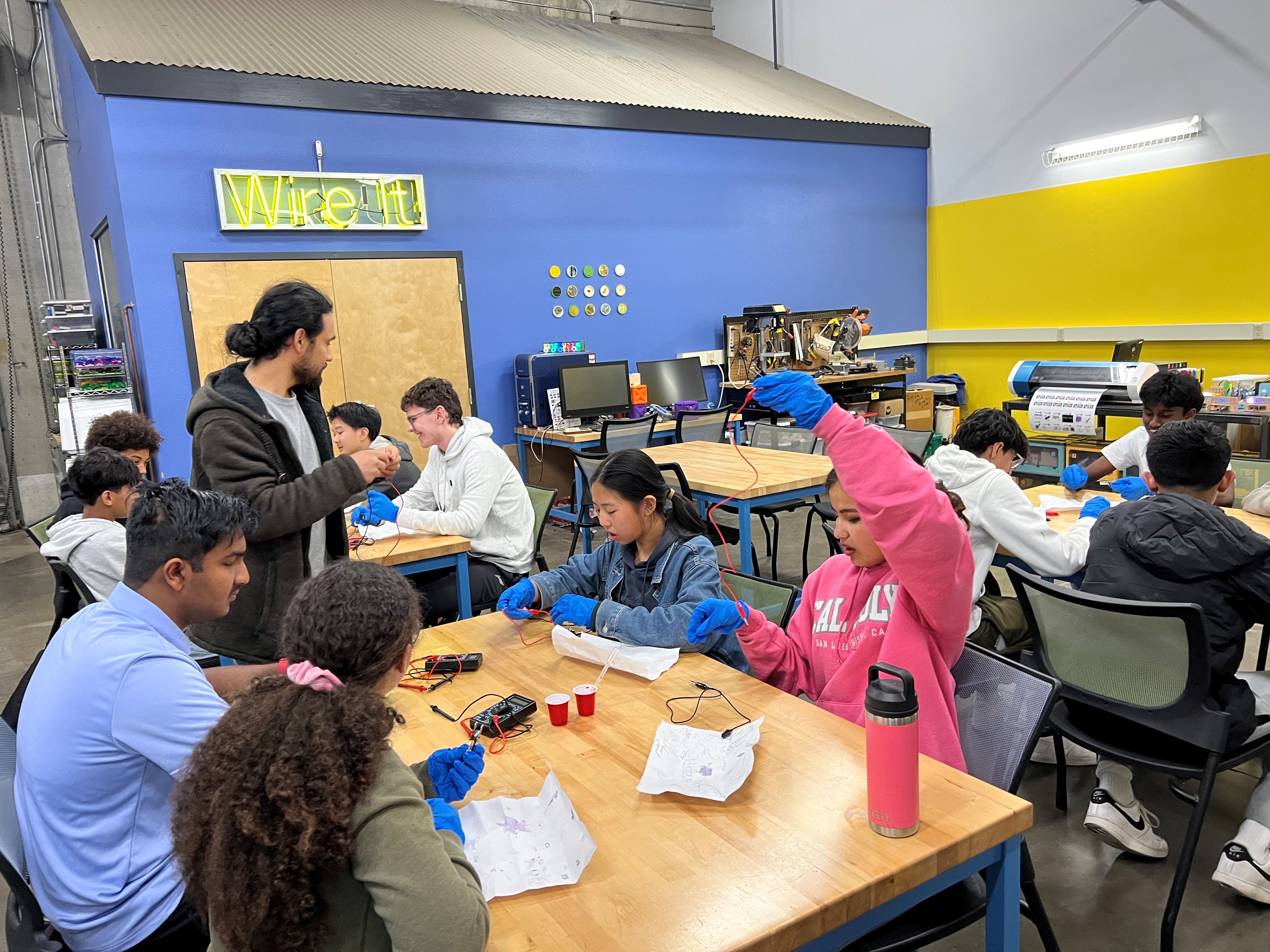
In collaboration with NSF BE-STARSE at UC Davis and SJCOE FabLab, we are launching a six-week Spring K-12 Workshop for 9th–12th grade students from the Greater Sacramento and Stockton areas. The program begins on March 8th and will run on Saturdays from 9 AM to 12 noon. UC Davis will host two sessions, while FabLab will host four. Throughout the program, UC Davis professors will give lectures on their fields of study and research. Students will engage in hands-on activities, including solar cell fabrication, Arduino-based projects, art and technology integration, and lab visits to the Cleanroom and other research facilities at UC Davis.
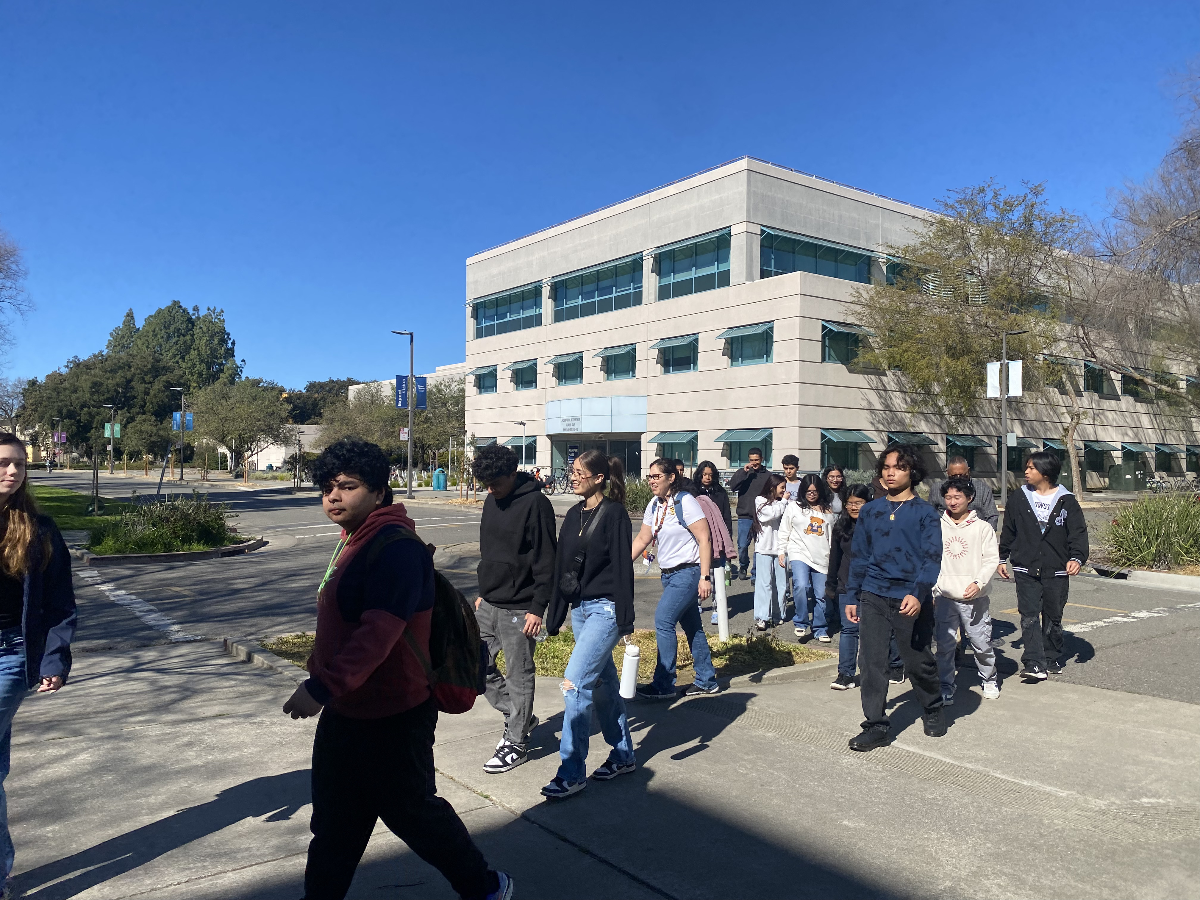
High School Field Trips to UC Davis
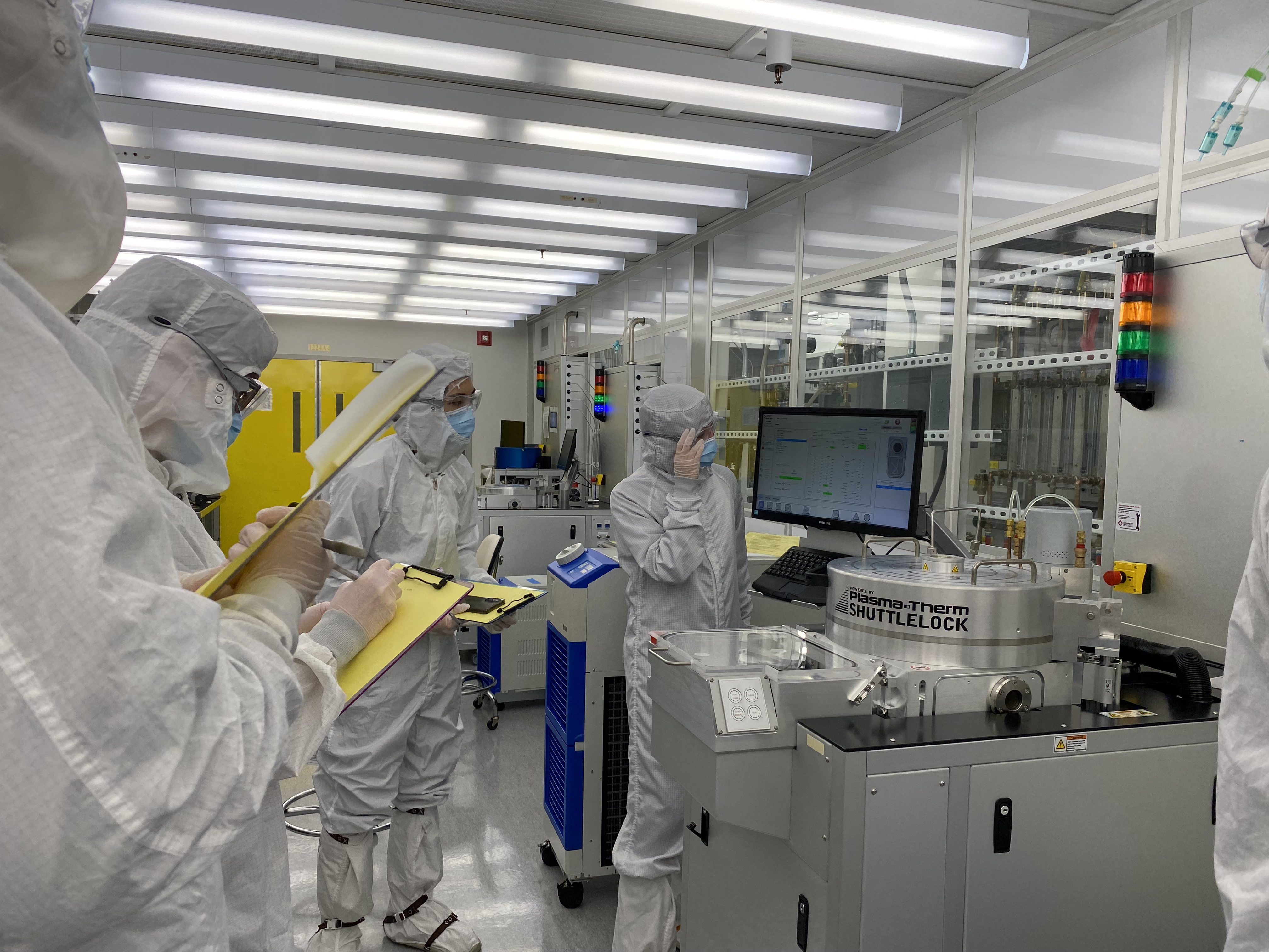
As part of the Northwest AI Hub’s collaboration with CITRIS INSPIRE, we have been hosting high school students from Stockton for field trips to UC Davis. The first visit took place on March 3rd with students from Edison High School, and the next will be on March 10th with students from Cesar Chavez High School. Each field trip includes three students who visit the Cleanroom, the Engineering Student Design Center (ESDC), and the Entomology Lab. Additionally, hands-on activities are arranged by UC Davis MESA students to provide an interactive learning experience.
Courses on Chip design and tape-out/manufacturing:
EEC 146A – Integrated Circuits Fabrication (seniors): This course covers the theory of microfabrication and uses the nanofabrication facility in UC Davis ( our university cleanroom) to process a CMOS circuit. Students observe the TAs and understand how microfabrication is done. Some fabrication steps use process simulation tools such as Silvaco. No commercial foundry tape-out is involved in this course.
EEC 289O: Design and Tape-out of Integrated Circuits (seniors and MS/PhD students): This course series involved layout design tools such as Cadence, Synopsys and PDKs of commercial foundries to design a CMOS and tape it out. After a commercial foundry completes the manufacturing and sends back to the students, it is tested by the students.